
ABOUT WAFERS
REQUEST A QUOTEInformation On Silicon Wafers
In electronics, a wafer (also called a slice or substrate) is a thin slice of semiconductor material, such as a silicon crystal, used in the fabrication of integrated circuits and other microdevices. The wafer serves as the substrate for microelectronic devices built in and over the wafer and undergoes many microfabrication process steps such as doping or ion implantation, etching, deposition of various materials, and photolithographic patterning. Finally the individual microcircuits are separated (dicing) and packaged.
Several types of solar cell are also made from such wafers. On a solar wafer a solar cell (usually square) is made from the entire wafer.
Formation
Wafers are formed of highly pure (99.9999999% purity) nearly defect-free single crystal material. One process for forming crystalline wafers is known as Czochralski growth invented by the Polish chemist Jan Czochralski. In this process, a cylindrical ingot of high purity monocrystalline semiconductor, such as silicon or germanium, is formed by pulling a seed crystal from a 'melt'. Donor impurity atoms, such as boron or phosphorus in the case of silicon, can be added to the molten intrinsic material in precise amounts in order to dope the crystal, thus changing it into n-type or p-type extrinsic semiconductor.
The ingot is then sliced with a wafer saw (wire saw) and polished to form wafers.
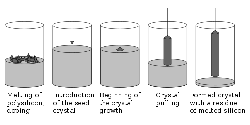
Illustration of the Czochralski process.
Wafer Properties
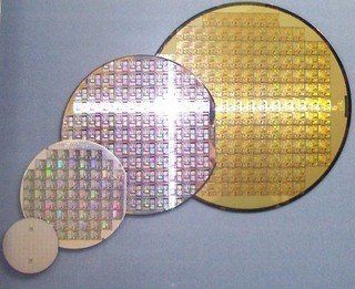
Silicon wafers are available in a variety of diameters from 25.4 mm (1 inch) to 450 mm (17.72 inches). Semiconductor fabrication plants (also known as fabs) are defined by the diameter of wafers that they are tooled to produce. The diameter has gradually increased to improve throughput and reduce cost with the current state-of-the-art fab considered to be 300 mm (12 inch), with the next standard projected to be 450 mm (18 inch).
- 1-inch (25 mm)
- 2-inch (51 mm). Thickness 275 µm.
- 3-inch (76 mm). Thickness 375 µm.
- 4-inch (100 mm). Thickness 525 µm.
- 5-inch (130 mm) or 125 mm (4.9 inch). Thickness 625 µm.
- 150 mm (5.9 inch, usually referred to as "6 inch"). Thickness 675 µm.
- 200 mm (7.9 inch, usually referred to as "8 inch"). Thickness 725 µm.
- 300 mm (11.8 inch, usually referred to as "12 inch"). Thickness 775 µm.
- 450 mm (17.7 inch, usually referred to as "18 inch"). Thickness 925 µm (expected).
Wafers grown using materials other than silicon will have different thicknesses than a silicon wafer of the same diameter. Wafer thickness is determined by the mechanical strength of the material used; the wafer must be thick enough to support its own weight without cracking during handling.
A unit wafer fabrication step, such as an etch step or a lithography step, can be performed on more chips per wafer as roughly the square of the increase in wafer diameter, while the cost of the unit fabrication step goes up more slowly than the square of the wafer diameter. This is the cost basis for shifting to larger and larger wafer sizes. Conversion to 300 mm wafers from 200 mm wafers began in earnest in 2000, and reduced the price per die about 30-40%.[14] However, this was not without significant problems for the industry.
Die Per Wafer Calculator
Uses inputs such as wafer diameter, die size, die spacing, and edge exclusion to calculate the total number of whole die per wafer
CALCULATOR
CRYSTALLINE ORIENTATION FLATS AND ORIENTATION NOTES
Wafers under 200 mm diameter have flats cut into one or more sides indicating the crystallographic planes of the wafer (usually a {110} face). In earlier-generation wafers had a pair of flats at different angles additionally conveyed the doping type (see illustration for conventions). Wafers of 200 mm diameter and above use a single small notch to convey wafer orientation, with no visual indication of doping type.
WAFER CRYSTALLOGRAPHIC ORIENTATION WAFER FLATS
One or two flats ground into the edge of the wafer indicate crystal orientation, and generally applies to wafers 125mm in diameter or smaller.
Flats can be used to denote doping and crystallographic orientation. Red represents material that has been removed.

CRYSTALLINE ORIENTATION FLATS AND ORIENTATION NOTCHES
Wafers are grown from crystals having a regular crystal structure, with silicon having a diamond cubic structure. When cut into wafers, the surface is aligned in one of several relative directions known as crystal orientations. Orientation is defined by the Miller index with (100) or (111) faces being the most common for silicon. Orientation is important since many of a single crystal's structural and electronic properties are highly anisotropic. Ion implantation depths depend on the wafer's crystal orientation, since each direction offers distinct paths for transport. Wafer cleavage typically occurs only in a few well-defined directions. Scoring the wafer along cleavage planes allows it to be easily diced into individual chips ("dies") so that the billions of individual circuit elements on an average wafer can be separated into many individual circuits.
About Dopants in Silicon
"IMPURITY"/DOPING
Silicon wafers are generally not 100% pure silicon, but are instead formed with an initial impurity doping concentration between 1013 and 1016 atoms per cm3 of boron, phosphorus, arsenic, or antimony which is added to the melt and defines the wafer as either bulk n-type or p-type. However, compared with single-crystal silicon's atomic density of 5×10²² atoms per cm3, this still gives a purity greater than 99.9999%. The wafers can also be initially provided with some interstitial oxygen concentration. Carbon and metallic contamination are kept to a minimum. Transition metals, in particular, must be kept below parts per billion concentrations for electronic applications.
Semiconductor doping is the process that changes an intrinsic semiconductor to an extrinsic semiconductor. During doping, impurity atoms are introduced to an intrinsic semiconductor. Impurity atoms are atoms of a different element than the atoms of the intrinsic semiconductor. Impurity atoms act as either donors or acceptors to the intrinsic semiconductor, changing the electron and hole concentrations of the semiconductor. Impurity atoms are classified as donor or acceptor atoms based on the effect they have on the intrinsic semiconductor.
CONDUTIVITY TYPE
An intrinsic semiconductor, also called an undoped semiconductor or i-type semiconductor, is a pure semiconductor without any significant dopant species present. The number of charge carriers is therefore determined by the properties of the material itself instead of the amount of impurities. In intrinsic semiconductors the number of excited electrons and the number of holes are equal: n = p.
An extrinsic semiconductor is a semiconductor that has been doped, that is, into which a doping agent has been introduced, giving it different electrical properties than the intrinsic (pure) semiconductor.
An n-type (negative-type) extrinsic silicon semiconductor is a semiconducting material that was produced by doping silicon with an n-type element of Group V A, such as P, As, or Sb. Consequently, electrons are the majority charge carriers of the material.
A p-type (positive-type) extrinsic silicon semiconductor is a semiconducting material that was produced by doping silicon with an p-type element of group III A, such as B, Al, or Ga. Since the dopants are acceptor atoms, holes are the majority charge carriers of the material.
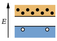
BAND STRUCTURE OF AN N-TYPE SEMICONDUCTOR
Dark circles in the conduction band are electrons and light circles in the valence band are holes. The image shows that the electrons are the majority charge carrier. Extrinsic semiconductors with a larger electron concentration than hole concentration are known as n-type semiconductors. The phrase 'n-type' comes from the negative charge of the electron. In n-type semiconductors, electrons are the majority carriers and holes are the minority carriers. N-type semiconductors are created by doping an intrinsic semiconductor with donor impurities (or doping a p-type semiconductor as done in the making of CMOS chips). In an n-type semiconductor, the Fermi energy level is greater than that of the intrinsic semiconductor and lies closer to the conduction band than the valence band.
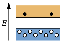
BAND STRUCTURE OF AN P-TYPE SEMICONDUCTOR
Band structure of a p-type semiconductor. Dark circles in the conduction band are electrons and light circles in the valence band are holes. The image shows that the holes are the majority charge carrier
As opposed to n-type semiconductors, p-type semiconductors have a larger hole concentration than electron concentration. The phrase 'p-type' refers to the positive charge of the hole. In p-type semiconductors, holes are the majority carriers and electrons are the minority carriers. P-type semiconductors are created by doping an intrinsic semiconductor with acceptor impurities (or doping a n-type semiconductor). P-type semiconductors have Fermi energy levels below the intrinsic Fermi energy level. The Fermi energy level lies closer to the valence band than the conduction band in a p-type semiconductor.
USES FOR EXTRINSIC SEMICONDUCTORS
Extrinsic semiconductors are components of many common electrical devices. A semiconductor diode (devices that allow current in only one direction) consists of p-type and n-type semiconductors placed in junction with one another. Currently, most semiconductor diodes use doped silicon or germanium.
Transistors (devices that enable current switching) also make use of extrinsic semiconductors. Bipolar junction transistors (BJT) are one type of transistor. The most common BJTs are NPN and PNP type. NPN transistors have two layers of n-type semiconductors sandwiching a p-type semiconductor. PNP transistors have two layers of p-type semiconductors sandwiching an n-type semiconductor.
Field-effect transistors (FET) are another type of transistor implementing extrinsic semiconductors. As opposed to BJTs, they are unipolar and considered either N-channel or P-channel. FETs are broken into two families, junction gate FET (JFET) and insulated gate FET (IGFET).
COMPOUND SEMICONDUCTORS
While silicon is the prevalent material for wafers used in the electronics industry, other compound III-V or II-VI materials have also been employed. Gallium arsenide (GaAs), a III-V semiconductor produced via the Czochralski process, is also a common wafer material.