Silicon Wafer Processing
SILICON WAFER PROCESSING
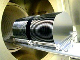
REQUEST A QUOTEAddison Engineering has an extensive array of processing capabilities. On our silicon or yours, we can provide virtually any processing service you may need, from a simple oxide layer to completely patterned wafers. All of the services listed below are available, from developmental lots to full production runs. Our goal is to provide our customer with the highest quality processing at competitive pricing. Whether you are a fabless company, need a specific process infrequently, or just need some extra capacity, let our staff unburden your process engineers.
REQUEST A QUOTE
- Oxide
- Thermal oxide
- TEOS/PETEOS oxide
- Gate oxide
- Low temperature oxide
- PSG glass
- Silicon Nitride
- LPCVD
- Low Stress
- Ultra-low Stress

- Polysilicon (undoped)
- Metal deposition: evaporation, sputter
- Epitaxial deposition
- Ion implantation
- SOI (oxidation, wafer bonding)
- Photolithography
- Photoresist: coat, strip
- Clean: RCA clean
- Mechanical:
- Ingot slicing
- Lap & etch
- Wafer thinning
- Wafer downsize (diameter cut-down)
- Wafer dicing
- Wafer reclaim
- Laser marking
- Wafer bumping
- MEMS - Silicon machining
CONTACT US
Have a question? Feel free to call us at 408-926-5000, or click the button below.
CONTACT US
Created by Olive + Ash.
Managed by Olive Street Design. ![]()